
450mm diameter research
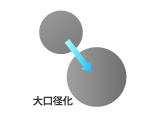
Highly integrated semiconductor devices as well as large-size 450mm diameter silicon wafers have brought about the need for high precision surface polishing for silicon wafers.
Fujimi stays ahead of next generation change in standards by concentrating product development on those wafer diameters expected to be most popular.
R&D facilities (Gifu Prefecture, Kagamigahara city)
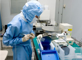
Our research and development facilities contain the same inspection and polishing equipment used by our customers (silicon wafer makers) to ensure research is proceeding in the right direction and the shift to full-production takes place as quickly and smoothly as possible.
Fujimi engineers undergo rigorous training to increase the speed of development efforts.